Fonon’s 3D Laser ZWLCT™ Glass Cutting Systems Have No Peers…

Fonon Technologies’ patented Zero Width Laser Cutting Technology (ZWLCT™) is a major discovery that remains the superior technology of choice today by Mother Glass Foundries. The demand for these systems remains high as new off-shore Flat Panel Display, Semiconductor and Electronic manufacturing facilities continue to emerge globally to support new market growth and cost reduction initiatives.
Zero Width Laser Cutting Technology has been optimized for thin-glass applications up to 1.0mm.
No other competing technology comes close to matching the superior performance of Fonon Technologies’ ZEROKerf™ glass cutting technology. Our patented process significantly increases edge quality and strength. Edge Impact Strength is increased up to 10 times when compared to full-contact mechanical scribe and break systems, while overall Glass Component Strength is improved up to 80%. ZWLCT™ splits materials at the molecular level under a non-contact process with tremendous speed resulting in no material loss, chips, lateral cracks, protrusions, hooks and flares or any other forms of contaminants.
ZWLCT™ eliminates surface degradation 100%, resulting in zero yield loss due to particulate damages across the glass surface caused by undesirable contaminates created by conventional mechanical scribe methods.

ZWLCT™

At the molecular level, Fonon Technologies’ patented ZWLCT™ generates a controlled MicroCrack™ to any selectable depth through glass (and other brittle materials) at a controlled, optimized angle to the surface of the material. By controlling the laser beam’s energy distribution under a proprietary temperature stress profile, the process creates scribe lines in a prescribed manner with no molecules leaving the surface of the glass, dramatically improving the substrate separation process.
The ZWLCT™ method incorporates cooling of the glass surface following controlled heating with the correct power density profile. This creates the intermolecular separation of the glass substrate to a predetermined depth.
Fonon Technologies’ 3D Laser ZWLCT™ Glass Cutting Systems can also be modified to enable the crossing of the laser cuts to provide a complete turnkey ZeroCut™ high-volume wafer dicing station.
Manufacturers and consumers benefit immediately from higher material strength as Fonon Technologies’ patented ZWLCT™ technology reduces production and handling damages at the factory while reducing premature latent product failures in the field due to shock.
Fonon Technologies optimizes each 3D Laser ZWLCT™ Glass Cutting System in response to continual advancements of customer applications.

Advantages of ZWLCT™ include:
- High cutting speed up to 1000 mm/sec
- Extremely high accuracy up to 10 microns achievable
- No post treatment of edges, such as grinding or edge seaming required
- Process unlimited component sizes up to Gen-10 and higher
- Easily adaptable to glass thickness changes during production
- Increased glass strength with no material loss or latent defects
- Excellent surface integrity of cut surface with no cracks or chips
- Precise edge geometries with almost any possible contour
- Edge Impact Strength up to 10X that of mechanical scribe & break methods
- Cut edges free of stress with Glass Component Strength improved 80%
 |
FLAT PANEL DISPLAY Processing Flat Panel Display Glass with ZWLCT™ technology improves edge impact strength up to 10 times and overall component strength up to 80% compared to conventional mechanical scribe methods. Fonon’s ZWLCT™ glass cutting systems reduce manufacturing costs, increase profit margins and dramatically increase yields providing a turnkey system that simultaneously laser scribes and breaks in one system. |
 |
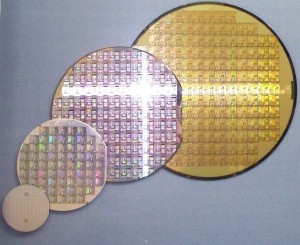
GLASS SEMICONDUCTOR WAFERS Wafers have the highest value at the dicing stage. It is critical from this point forward through the rest of the manufacturing process to maintain the highest yields and die count. Wafer Carriers, LEDs, Optical Sensors & Detectors, CMOS Image Sensors and Bonding Silicon-On-Insulators to glass wafers incorporating ZWLCT™ allow closer die spacing increasing the number of die/wafer. With no material breaching or fissures, yields are dramatically improved lowering production costs while eliminating potential latent field failures. |


